|
To view online, please click here.
SEM | TEM | EPMA | Sample Prep | NMR | Mass Spec | FIB | E-Beam | Elemental Analysis
|
 |
|
JEOL USA Microscopy News
|
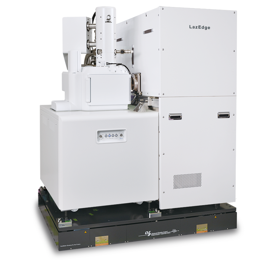
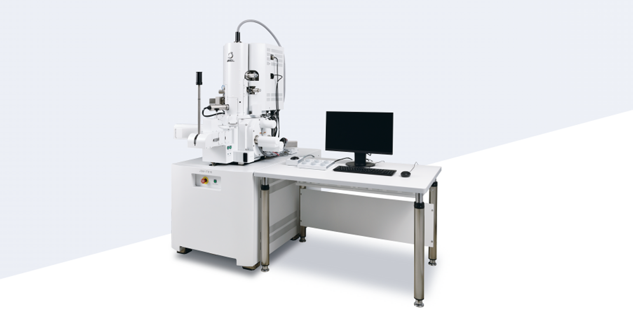
Launch of the Laser SEM System "LazEdge"
|
 |
|
JEOL's LazEdge integrates a laser processing system directly inside the SEM specimen chamber, enabling large-area cross-sectional preparation without breaking vacuum. The result is a seamless, contamination-free workflow from sample preparation to high-resolution SEM observation in a single uninterrupted session.
LazEdge produces cross-sections ready for EBSD analysis. It is well-suited for metals, semiconductors, and battery materials. Explore the system and reach out to the JEOL team to discuss your application.
|
| Explore LazEdge |
|
|
|
EPMA User Meeting 2026
|
 |
|
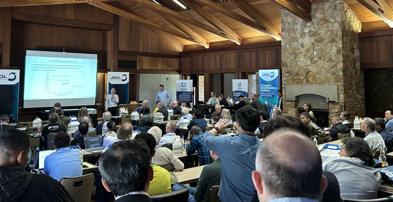
JEOL is hosting the 2026 EPMA User Meeting, September 22-24 at the Stanford Deep Lab, a new state-of-the-art shared analytical facility at Stanford University. This focused gathering brings together electron probe microanalysis researchers and practitioners for technical and keynote presentations, including speakers from the Americas EPMA community, hands-on sessions on next-generation EPMA technologies, and direct engagement with JEOL's R&D, Service, and Applications teams.
Whether you are a current JEOL EPMA user or an electron probe researcher looking to connect with the community, this is an event worth attending. Registration is limited to the first 30 attendees, and if you'd like to present, you can register for a Lightning Talk to showcase your research. Reserve your spot today.
|
| Register Now |
|
|
|
Solving Unknown Crystal Structures with JEOL's YOKOGUSHI Approach
|
 |
|
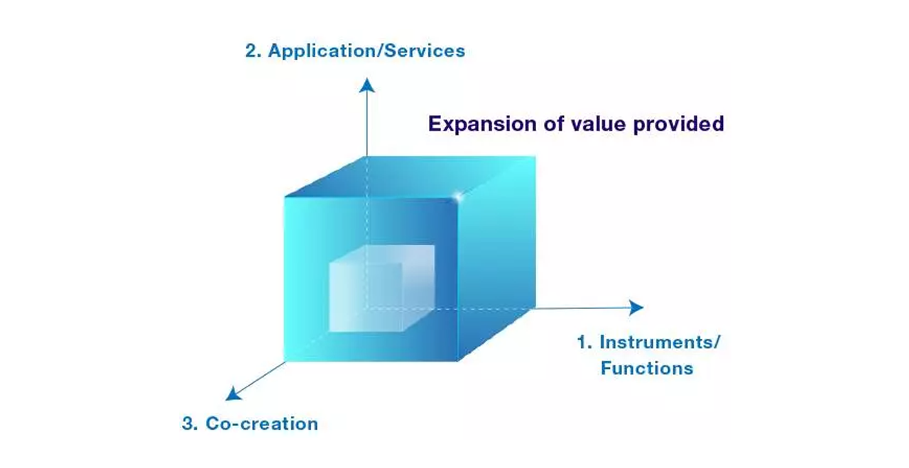
Some analytical challenges cannot be solved by a single instrument. JEOL's YOKOGUSHI cross-platform analysis strategy combines instruments, applications, and co-creation with research partners to deliver solutions beyond what any single technique can achieve.
A recent application note demonstrates this in action: determining the complete crystal structure of a nano-crystalline powder with no prior structural information, by integrating 3D electron diffraction, high-resolution mass spectrometry, database mining, quantum chemical computation, and solid-state NMR.
Explore the full range of YOKOGUSHI applications and see how cross-platform analysis can advance your research.
|
| Read Application Note |
|
|
|
Automation of High-Magnification Observation of NMC Cathode Active Material
|
 |
|
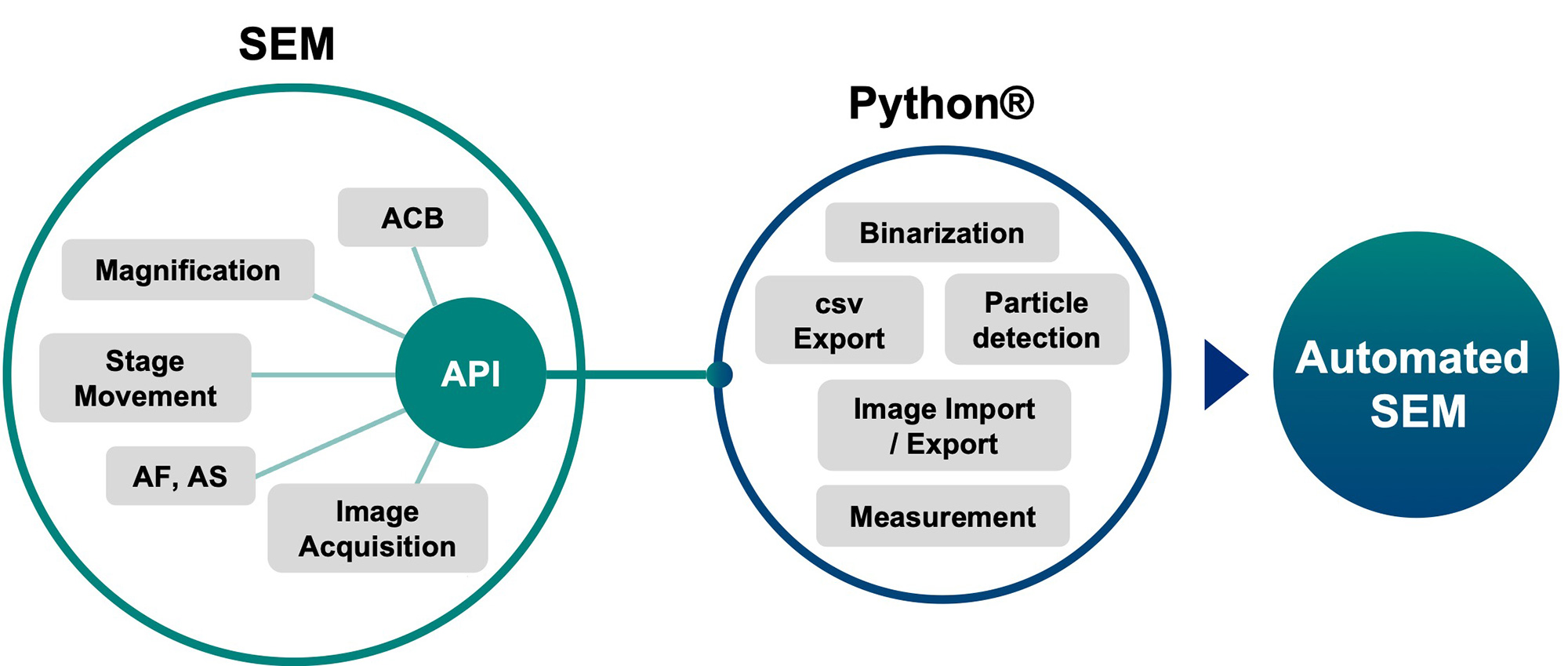
Consistent, high-throughput characterization of NMC cathode active material is central to battery materials research and quality control. This application note demonstrates how JEOL's automated SEM workflow, built on the SEM External Control API and Python, enables systematic high-magnification observation of NMC particles, reducing operator variability and improving data reproducibility.
The automated approach captures particle morphology, size distribution, and surface detail across a statistically representative sample set. Read the application note to review the full methodology and results.
|
| Read Application Note |
|
|
|
Celebrating 35 Years of JEOL de Mexico
|
 |
|
This year marks a significant milestone for our colleagues to the south. JEOL de Mexico is celebrating 35 years of delivering scientific instrumentation and technical support to research institutions and industry throughout the country. Since 1991, the team has contributed to scientific advancement across electron microscopy, analytical chemistry, and materials characterization.
We congratulate everyone at JEOL de Mexico on this achievement. Here's to 35 years of precision, partnership, and scientific progress.
|
|
|
|
JEOL USA Image Contest
|
 |
|
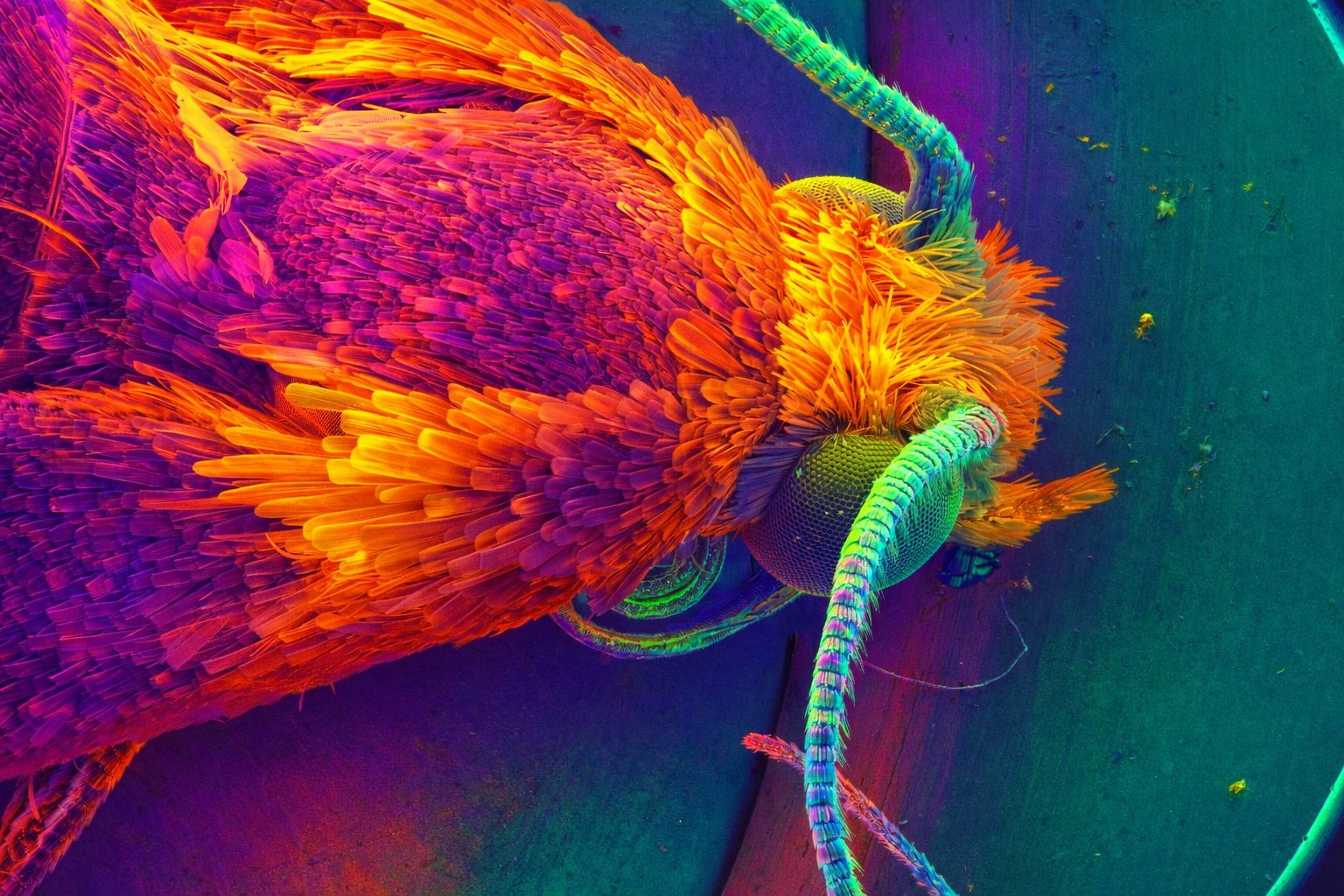
Have a striking micrograph captured on your JEOL instrument? The JEOL USA Image Contest is open year-round for submissions from users of SEM, TEM, EPMA, and other JEOL systems. Each month, our team selects a winner from submitted entries and recognizes them across our community.
Monthly winners receive a $200 Amazon gift card and a custom e-certificate. Submit your image and share the science behind it.
|
| Submit Your Image |
|
|
|
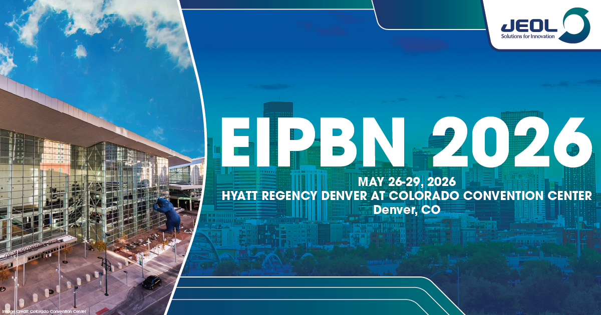
JEOL at EIPBN 2026
|
 |
|
The JEOL JBX team joined the 2026 International Conference on Electron, Ion, and Photon Beam Technology and Nanofabrication (EIPBN), May 26-29 in Denver, Colorado, showcasing the latest in e-beam lithography for nanofabrication and semiconductor research.
EIPBN brings together leading researchers, engineers, and developers working at the intersection of advanced patterning and beam technology. Connect with the JEOL JBX team to learn more about our e-beam lithography solutions.
|
|
|
|
Webinar: Basics of SEM Array Tomography
|
 |
|
JEOL is hosting an on-demand webinar covering the fundamentals of SEM Array Tomography, a volume electron microscopy (vEM) technique that uses serial sectioning and automated SEM imaging to generate three-dimensional data from tissue and other biological specimens. The session is designed for researchers interested in adding array tomography to their workflow, or those navigating challenges with serial sectioning and sample preparation.
The webinar is available June 24-26, 2026 (JST). Registration is free.
|
| Register Now |
|
|
|
|
|
|